
Diffraction
Structure Analysis by Precession Electron Diffraction Tomography (PEDT)
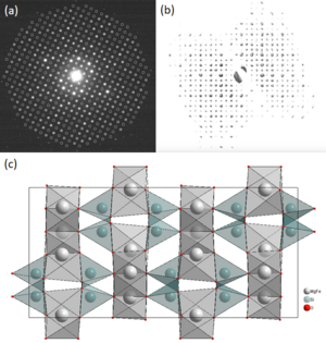
Structure solving of unknown phases at the nanometre scale in a TEM is now possible. The method is based on the tomographic acquisition of 3D precession electron data followed by quantitative analysis of intensities, as currently done using adhoc softwares for X-Ray diffraction data. Structure refinement is also possible thanks to the dynamical calculation of intensities and comparison with experimental data. In the figure (a) Precession electron diffraction pattern and its quantitative treatment for 3D reconstruction. (b) 3D reconstruction of PED data. (c) Orthopyroxene structure as solved and refined by PEDT. Mg and Fe fractioning of octahedral sites is quantified (Palatinus et al., 2015, Rondeau et al., 2019).
Damien Jacob (MTP-UMET), Pascal Roussel (MISSP-UCCS), Lukáš Palatinus (Laboratory of Electron Crystallography, Institut of Physics, Czech Academy of Sciences)
Crystallographic identification by PED and CBED
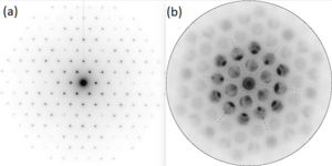
Space group determination of unknown phases is achieved in two steps: (i) Analysis of the symmetry of zone-axes PED patterns for the so-called “extinction symbol” determination. The analysis is done by comparing experimental data with theoretical ones as calculated for all possible space-groups and tabulated in a Diffraction Atlas written by J P. Morniroli (see http://electron-diffraction.fr/). (ii) Analysis of the symmetry of zone-axes CBED patterns for the so-called “diffraction group” determination and subsequent deduction of the point group. In the figure (a) PED pattern as taken on a low-temperature quartz sample. Pattern symmetry symbol is 6mm. (b) CBED pattern as taken on a low-temperature quartz sample. Pattern symmetry symbol is 3m (Morniroli et al., 2012, Jacob et al., 2012).
Damien Jacob (MTP-UMET), Gang Ji (MPGM-UMET), J.P. Morniroli
Phase and orientation mapping by STEM-diffraction (4D STEM)
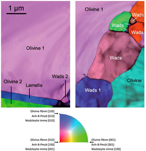
Phase and orientation mapping by STEM-diffraction (or Automated Crystal Orientation Mapping, ACOM) as obtained in a TEM gives similar results to those obtained by EBSD in a SEM. The method enables the microstructure analysis with nanometre resolution on a sample area scanned with a small converging electron probe (a few nanometer in size). Automated analysis is done by comparing experimental patterns with simulated ones for all possible orientations of the crystal. In the figure: microstructure analysis of an olivine sample as deformed at high pressure and temperature. Orientation relationships between the phases formed during the transformation clearly appear (examples: Nzogang et al., 2018, Nzogang et al., 2018, Addad et al., 2019, Nzogang et al., 2020).
Damien Jacob (MTP-UMET), Alexandre Mussi (Plasticité-UMET), Ahmed Addad (UMET), Patrick Cordier (Plasticité-UMET)