
Functional Oxides
Microstructural characterization of oxide thin films used in nano-devices
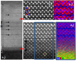
The development of new materials in the form of thin oxide layers, which can be integrated into nano-devices for electronics and optics or used in the energy field, is essential. Thus establishing the relationships between the microstructure and the physical properties in order to optimize their performance requires the use of transmission electron microscopy. Let us take the example of an Nd2Ti2O7 layer (a form) on a STO 110 substrate. We see on the HAADF image of the entire layer (a1) a clear band of about 2.1 nm near the interface as well as defects indicated by black arrows. An enlargement of the image far from the interface (a2) shows a perfect superposition of the [100] projection of the NTO structure. EDS mapping (a3) confirms the position of the ions without diffusion phenomenon. An enlargement of the image near the interface at the level of the clear band (a4) and the EDS cartography (a5) makes it possible to attribute the clearer contrast to the replacement of the Sr ions by Nd.
Understanding the oxygen storage mechanisms in YbFe2O4 +x (x ≤ 0.5)
The search for new functional materials is more relevant than ever in the current energy context. As such, the conception and the crystallo-chemistry of new inorganic phases with remarkable properties is essential.
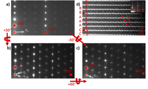
For example, the RFe2O4 compounds are multiferroic and after oxidation, these compounds are known to admit a significant amount of interstitial anions in their structure (up to 0.5 oxygen per form unit). For the first time, by combining different techniques, the immeasurable modulated crystal structure was solved and the structural model of YbFe2O4+x was completely understood by the localization, in particular of interstitial oxygen. Modulation phenomena were identified by transmission electron microscopy. Indeed, the study by electronic diffraction reveals the presence of two types of satellites with two very different origins. The first is characterized by very low intensity spots observed along the zone axis [-110]h (fig. a) and corresponds to the modulation vector q2,YbFe2O4.5 ≈ 0.36 ah* + 0.36 bh* where h refers to the basic hexagonal mesh of the compound YbFe2O4+x. The main satellites appear in the zone axis [010]h (fig. b), but also after rotation around the axis [100]h (fig. c). They correspond to the modulation vectors q1,YbFe2O4.5 et q1T= ~0.27 ah* + ~0.36 ch*. In the HAADF image (fig. d) the most intense points correspond to the Yb and the least intense to the Fe. It shows a periodic undulation every 3 ytterbium cations in rows of about three atoms as well as stacking faults indicated by red arrows (Nicoud et al., 2017).
Sarah Nicoud (MISSP-UCCS), Marielle Huvé (MISSP-UCCS), Olivier Hernandez (ISCR, Université de Renne), Alain Pautrat (CRISMAT, Caen), Mathieu Duttine (ICMCB, Université Bordeaux), Alain Wattiaux (ICMCB, Université Bordeaux), Claire Colin (Institut NEEL, Université Grenoble Alpes), Houria Kabbour (MISSP-UCCS), Olivier Mentré (MISSP-UCCS)