
Semiconductors/Microelectronics
Structure of sputtered pseudocapacitive vanadium nitride films
Vanadium Nitride is a very promising pseudocapacitive material (Robert et al., 2018). Compatible with production sputtering techniques it can be considered for potential applications in the conception of miniaturized power sources. As part of a larger study aiming to understand the charge storage process of this promising pseudocapacitive material (Robert et al., 2020), we have performed a multiscale electron microscopy investigation of the morphology, structure and electronic properties of vanadium nitride/Si heterostructures prepared by vapor deposition methods.
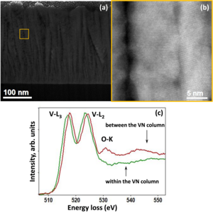
In the figure HAADF images of VN layer deposited on silicon wafer can be seen. Both images show columnar growth of the VN with a feather-like morphology of the VN columns. The interplanar distances in the columns correspond to stoichiometric VN film The darker regions observed in the images correspond the regions between the VN pillars where those spaces can be attributed either to porosities or oxidized regions. In order to elucidate the nature of the inter-column regions we investigated the ELNES structures of the N-K (not shown) and the V-L3,2 edges. For the V-L3 edge a shift towards higher energies (of about 0.75 eV) occurs between the VN columns and a clear appearance of the O-K edge. These observations clearly indicate the formation of a vanadium oxide (VO2) at the interface between the VN columns. In very few case the formations of V2O3 oxides has been identified. Some minor formations of V2N or V2NxOy has also been identified. TEM images reveal that the vanadium oxides are in amorphous state.
Marielle Huvé (MISSP-UMET), Kevin Robert (CSAM- IEMN), Christophe Lethien (CSAM- IEMN), Maya Marinova (PMEL), David Troadec (IEMN), Pascal Roussel (MISSP-UMET)